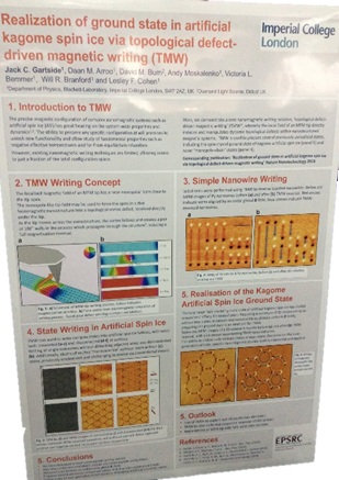
Realization of ground state in artificial kagome spin ice via topological defect-driven magnetic writing
J.C. Gartside, D.M. Arroo, D.M. Burn, A.V. Moskalenko, V.L. Bemmer, L.F. Cohen and W.R. Branford
IoP Magnetism Manchester Apr 2018
Arrays of non-interacting nanomagnets are widespread in data storage and processing. As current technologies approach fundamental limits on size and thermal stability, enhancing functionality through embracing the strong interactions present at high array densities becomes attractive.
In this respect, artificial spin ices[1-4] are geometrically frustrated magnetic metamaterials that offer vast untapped potential due to their unique microstate landscapes, with intriguing prospects in applications from reconfigurable logic to magnonic devices6 or hardware neural networks[7].
However, progress in such systems is impeded by the inability to access more than a fraction of the total microstate space. To address this, we have developed a novel scanning probe technique, Topological DefectDriven Magnetic Writing (TMW)[5] , which provides full access to all possible microstates in artificial spin ices and related arrays of nanomagnets.
We employ TMW to create previously elusive magnetic configurations such as the spin- crystal ground state[8] of artificial kagome dipolar spin ices and high-energy, low-entropy monopole-chain states that exhibit negative effective temperatures.

Figure 1: i)Micromagnetic simulation and accompanying schematic of writing process dynamics showing positions of magnetic charges (±Q). ii) MFM image of ladder and zigzag monopole-defect chain states written at RT on a NiFe ASI lattice. iii) MFM image of the spin-crystal chiral ground state of kagome ASI written at RT on a NiFe ASI rosette.
[1] Wang, RF, et al. Nature 439.7074 (2006): 303-306.
[2] Branford, W. R., et al. Science 335.6076 (2012): 1597-1600.
[3] Zhang, Sheng, et al. Nature 500.7464 (2013): 553-557.
[4] Perrin, Yann, et al. Nature 540.7633 (2016): 410-413.
[5] Gartside, J. C., et al. Nature Nanotechnology 13 (2017): 53-58.
[6] Heyderman, L. J., and R. L. Stamps. J. Phys.: Cond. Matt. 25.36 (2013): 363201.
[7] Wang, Yong-Lei, et al. Science 352.6288 (2016): 962-966.
[8] Anghinolfi, L., et al. Nat. Comms. 6 (2015).