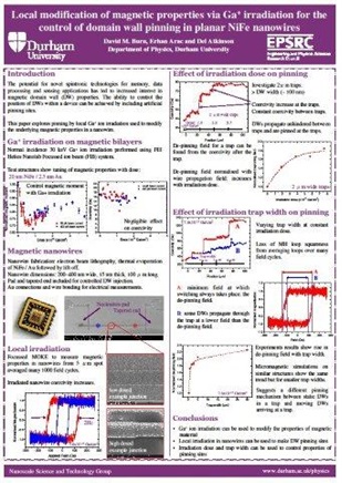
Local modification of magnetic properties via Ga+ irradiation for the control of domain wall pinning in planar NiFe nanowires
D.M. Burn, E. Arac and D. Atkinson
Joint European Magnetic Symposia Parma, Italy Sep 2012
The control of domain walls in magnetic nanowires is a popular research theme as their use in spintronic devices for memory, sensing and logic processing applications grows. In such devices information is represented by the magnetisation direction of regions of the nanowire separated by domain walls. To achieve high density devices, controlling the pinning of these domain walls is essential.
Domain wall pinning has previously been achieved by modifying the structural geometry of the wire with notches or anti-notches [1]. Here we show that domain wall pinning behaviour can be achieved through local modifications to the underlying magnetic material of the nanowire through focussed Ga+ ion irradiation. With this technique the positioning and the potential energy of the pinning sites can be controlled without the need for lithographic structuring.
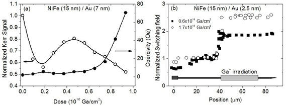
A detailed investigation has been performed on the magnetic changes (Fig 1(a)) taking place within NiFe / Au bilayers as a result of low dose irradiation induced interfacial intermixing [2]. This has revealed that fine control over the saturation magnetisation can be achieved for low dose irradiation. Localised control of domain wall pinning using irradiation induced intermixing has been demonstrated in nanowires here (Fig 1(b)). Furthermore, this approach could also potentially lead to a reduction in the critical current density for current induced domain wall motion when Ga+ irradiated pinning sites are used [3].

Magnetic properties of Ga+ irradiated NiFe / Au bilayer (a) structures and (b) nanowires.
[1] L.K. Bogart et.al., Phys. Rev. B 79, 054414 (2009).
[2] E. Arac et.al., J. Appl. Phys. 111, 044324 (2012).
[3] K.J. Lee et. al., J. Magn. Magn. Mater. 304, 102 (2006).